The Black Pill (STM32F411CEU6)

In this article, we will get you started with the STM32F411CE board (aka the black pill). For a complete overview of the board see this.
This chip is based on ARM Cortex-M4 32-Bit Architecture with clock frequency of 100 MHz RAM of 512KB.
This chip is manufactured by the Dutch company STMicroelectronics, which is based in Switzerland. The company provides several tools to develop for their chips. The official IDE is called the STM32CUBE IDE which is used for this quick tutorial.
1. Getting Started
1.1. Overview
The illustration below demonstrates the characteristics of the pins on the board.

1.2. Requirements
-
Development Environment: You can choose either of the following:
- STM32Cube IDE:
This is the official STM32 IDE and it includes build environment. you can download it from here.
-
CMake and Custom IDE:
Assuming you have CMake installed.
-
Download the GNU Arm Embedded Toolchain from here and add it to
PATH. This is important to compile the project. -
Download the OpenOCD from here and add it to
PATH. This is important for debugging. -
Download the STM32CubeMX from here and add it to
PATH. This is important to generate the project files along HAL library.
-
-
STM32 Cube Programmer: To upload the binary to the chip. You can download it from here.
1.3. Setting up the environment
1.4. Setting Up the Clock
Set HSE and LSE to crystal clock on the RCC. Now we will configure the clock depending on the chip. For example, the STM32F411CEUx from Weact is connected to a $32.786$ kHz resonator on the LSE and a 25 MHz resonator on the HSE, so the configuration diagram should be like this:
- Set PPL Source Mux to HSE
- Set
/M=/ 25 - Set
*N=X 192 - Set
/Q=/ 4 - Set
/P=/ 2 - Set System Clock Mux to PLLCLK
- Set
AHB Prescaler=/ 1
Notice that the STM32F411CEUx supports up to 100 MHz clocking, but since the Universal Serial Bus On-The-Go Full Speed (USB_OTG_FS) requires a dedicated 48 MHz clock (datasheet 3.27), the clock responsible for this (48 MHz clocks) comes from the Main PLL directly. By clocking the HCLK to 96 MHz, we can achieve a division that results in 48 MHz for this clock.
2. Project Structure
2.1. Project Settings (myproject.ioc)
This file defines the settings of the chip when it starts, and the necessary code is re-generated whenever this file is updated. From here, you can set the initial mode of the pins (input. output, etc…), Direct Memory Access (DMA) settings, timers and more.
2.2. Linker Script (STM32F411CEU6_FLASH.ld)
Let’s take a look at the linker script generated by STM32 Cube MX:
/* Entry Point */
ENTRY(Reset_Handler)

/* Highest address of the user mode stack */
_estack = ORIGIN(RAM) + LENGTH(RAM);    /* end of RAM */
/* Generate a link error if heap and stack don't fit into RAM */
_Min_Heap_Size = 0x200;      /* required amount of heap  */
_Min_Stack_Size = 0x400; /* required amount of stack */

/* Specify the memory areas */
MEMORY
{
RAM (xrw)      : ORIGIN = 0x20000000, LENGTH = 20K
FLASH (rx)     : ORIGIN = 0x08000000, LENGTH = 64K
}
/* ... */
In the linker script (STM32F411CEU6_FLASH.ld), the ENTRY(Reset_Handler) directive specifies this entry point.
The Reset_Handler is the entry point for the program and is defined in the assembly file startup_stm32f103xb.s.
- It is responsible for initializing the system and preparing the execution environment before jumping to the main application code.
- When the microcontroller is reset, the
Reset_Handleris the first function that gets executed as specified in the above linker. - This handler is crucial in setting up the system by configuring the stack pointer, initializing data segments, and calling the
main()function.
2.2.1. Memory Layout
The memory configuration is defined in the linker script under the MEMORY section. This section specifies the start addresses and lengths of different memory regions in the microcontroller:
- RAM: The RAM region is defined with a starting address of
0x20000000and a length of 20KB. This is the area where the runtime data (variables, stack, and heap) will be stored. - FLASH: The FLASH region, starting at
0x08000000with a length of 64KB, is used to store the program code and constants.
2.2.2. Stack and Heap Configuration
-
_estack: The
_estacksymbol defines the highest address of the stack in RAM. It is calculated as the sum of the starting address of RAM (ORIGIN(RAM)) and the total length of RAM (LENGTH(RAM)). This ensures that the stack starts at the end of the available RAM space and grows downwards. -
_Min_Heap_Size: This value specifies the minimum required heap size, which is set to
0x200(512 bytes). The heap is used for dynamic memory allocation during runtime. -
_Min_Stack_Size: This value defines the minimum required stack size, set to
0x400(1024 bytes). The stack is used for storing local variables and function call information during execution.
These values ensure that the heap and stack have enough space within the RAM, preventing overlap and potential runtime errors. The linker script will generate an error if the specified heap and stack sizes do not fit within the defined RAM area.
2.3. C Entry File (core/Src/main.c)
This is the main source code, where the entry function resides. Also, this is place where most of the generated code done by the IDE is written after updating myproject.ioc.
We will look into two important functions here.
2.3.1. static void MX_GPIO_Init(void)
This function sets up the initial settings for the IO pins of the chip. On the board the blue LED is connected to pin C13. If we set this pin mode to GPIO_Output mode in the myproject.ioc file, as in the illustration below
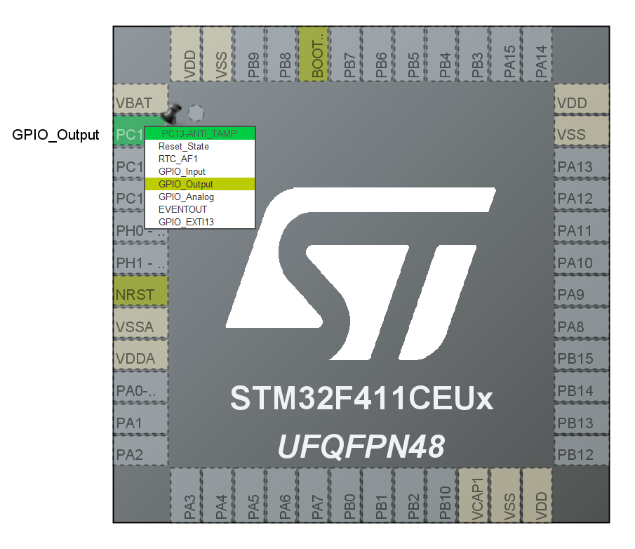
Figure 2: Configuring the chip’s pins
we can see that the IDE has generated the following code in the function MX_GPIO_Init:
GPIO_InitTypeDef GPIO_InitStruct = {0};

/* GPIO Ports Clock Enable */
__HAL_RCC_GPIOC_CLK_ENABLE();

/*Configure GPIO pin Output Level */
HAL_GPIO_WritePin(GPIOC, GPIO_PIN_13, GPIO_PIN_RESET);

/*Configure GPIO pin : PC13 */
GPIO_InitStruct.Pin = GPIO_PIN_13;
GPIO_InitStruct.Mode = GPIO_MODE_OUTPUT_PP;
GPIO_InitStruct.Pull = GPIO_NOPULL;
GPIO_InitStruct.Speed = GPIO_SPEED_FREQ_LOW;
HAL_GPIO_Init(GPIOC, &GPIO_InitStruct);
Lines from 9 to 14 are responsible for initializing the pin C13. We can see in line that the HAL library provides the function HAL_GPIO_Init which takes first the name of the Pins block and then a pointer to a structure GPIO_InitTypeDef. This is also how the pin settings is changed programmatically. The details of the pins settings are explained in the following section.
The Pull variable specifies which resistors should be connected to the pin. The possible configurations are
- Pull down (
GPIO_PULLDOWN) - Pull up (
GPIO_PULLUP) - No resistor (
GPIO_NOPULL)
The pull down resistor connects the pin to the ground, while the pull up resistor connects the pin to 3.3V.
3. Uploading Firmware
Uploading firmware to an STM32 microcontroller can be achieved using different interfaces such as DFU (Device Firmware Upgrade) or UART. Below are the steps for using both methods with the WeAct Black Pill board.
3.1. Using DFU Mode
To upload the firmware via DFU mode, connect your device via USB and use the following command:
STM32_Programmer_CLI -c port=usb1 -w \Debug\app.bin 0x08000000
port=usb1: Specifies the USB port.-w \Debug\app.bin: Indicates the path to the binary file.0x08000000: Specifies the start address in the flash memory.
3.2. Using UART
To upload the firmware via UART, use the following command:
STM32_Programmer_CLI -c port=COM10 -w \Debug\app.elf
port=COM10: Specifies the COM port.-w \Debug\app.elf: Indicates the path to the ELF file.
To reset and disable the read protection of the microcontroller, you can use:
STM32_Programmer_CLI -c port=COM10 -rdu
4. Working with GPIOs
GPIO (General Purpose Input/Output) is crucial for interfacing with the STM32 microcontroller’s pins. Below is an overview of how to configure and use GPIOs.
4.1. GPIO Initialization (GPIO_InitTypeDef)
GPIO_InitTypeDef is a structure used to define the specifications of a GPIO pin. Below are the key fields in this structure:
typedef struct
{
  uint32_t Pin;
  uint32_t Mode
  uint32_t Pull;
  uint32_t Speed;
  uint32_t Alternate; // Only available in >= Cortex-M4
} GPIO_InitTypeDef;
-
Pin: Specifies the GPIO pins to be configured. Multiple pins can be selected using a bitwise OR operation. Example:(GPIO_PIN_0 | GPIO_PIN_1). Mask of the pin,(GPIO_PIN_0 = 0x0001),(GPIO_PIN_1 = 0x0002)… Mode: Defines the operating mode for the selected pins. The following modes are available:- Input Mode
GPIO_MODE_INPUT:Input Floating ModeThe input mode changes a variable variable according to the voltage applied to the pin (Note this should never exceed 3.3V for most pins).
- Output Mode
GPIO_MODE_OUTPUT_PP:Output Push-PullThe push-pull mode sets up the pin for a single direction output. The pin state, can either be high or low.
GPIO_MODE_OUTPUT_OD:Output Open DrainThe open-drain mode, sets up the pin to accept bidirectional input and output. (For more see this article).
- Alternate Function
GPIO_MODE_AF_PP:Push-PullGPIO_MODE_AF_OD:Open Drain
- Analog Mode
GPIO_MODE_ANALOG:Analog ModeThe analog mode allows the pin to read the voltage applied to it. However, not all pins are able to be set to this mode, in the case of this chip, these pins are A0..A7 as well as B0 and B1, which also correspond to ADC0..ADC9. Accessing the analog value read from the pin needs additional configuration, such as direct memory access (DMA), which we will look into in the following sections.
- External Interrupt
GPIO_MODE_IT_RISING:Rising EdgeGPIO_MODE_IT_FALLING:Falling EdgeGPIO_MODE_IT_RISING_FALLING:Rising and Falling Edge
- External Event
GPIO_MODE_EVT_RISING:Rising EdgeGPIO_MODE_EVT_FALLING:Falling EdgeGPIO_MODE_EVT_RISING_FALLING:Rising and Falling Edge
- Input Mode
Pull: Specifies the internal pull-up or pull-down resistor activation:GPIO_NOPULL: No pull-up or pull-down activation.GPIO_PULLUP: Pull-up resistor activation.GPIO_PULLDOWN: Pull-down resistor activation.
Speed: Defines the speed for the GPIO pin:GPIO_SPEED_FREQ_LOW: 2 MHz.GPIO_SPEED_FREQ_MEDIUM: 12.5 to 50 MHz.GPIO_SPEED_FREQ_HIGH: 25 to 100 MHz.GPIO_SPEED_FREQ_VERY_HIGH: 50 to 200 MHz.
An example of initializing a pin:
GPIO_InitTypeDef GPIO_InitStruct = {};
GPIO_InitStruct.Pin = GPIO_PIN_13;
GPIO_InitStruct.Mode = GPIO_MODE_OUTPUT_PP;
GPIO_InitStruct.Pull = GPIO_NOPULL;
GPIO_InitStruct.Speed = GPIO_SPEED_FREQ_LOW;
HAL_GPIO_Init(GPIOC, &GPIO_InitStruct);
4.2. GPIO Pin States (GPIO_PinState)
A GPIO pin can be in one of the following two states:
- Reset State (
GPIO_PIN_RESET): Logical low (0). - Set State (
GPIO_PIN_SET): Logical high (1).
4.2.1. Writing to a Pin
To set or reset a GPIO pin, you can use the following methods:
Setting a Pin
GPIOA -> BSSR = GPIO_PIN_0;                         // fast
GPIOA -> ODR |= GPIO_PIN_0;                         // legacy
HAL_GPIO_WritePin(GPIOA, GPIO_PIN_0, GPIO_PIN_SET); // HAL Library
Resetting a Pin
GPIOA -> BSSR = (uint32_t)GPIO_PIN_0  << 16U;         // fast
GPIOA -> ODR &= ~GPIO_PIN_0;                          // legacy
HAL_GPIO_WritePin(GPIOA, GPIO_PIN_0, GPIO_PIN_RESET); // HAL Library
No Masking needed for setting/resetting a pin when using BSRR register, ODR Registers stores the output values and we can use it to read the output values.
Note that the function HAL_GPIO_WritePin writes the value to the pin atomically without OR’ing it with other masks. That means interrupts do not have to be disabled.
4.2.2. Reading a Pin
Just like reading the Output data from ODR, we can read the input data from IDR.
uint8_t PA0;
PA0 = GPIOA -> IDT & GPIO_PIN_0;            // legacy
PA0 = HAL_GPIO_ReadPin(GPIOA, GPIO_PIN_0);  // HAL Library
4.3. GPIO Port Configuration (GPIO_TypeDef)
Each GPIO port is represented by a GPIO_TypeDef structure, which contains the following registers:
typedef struct
{
  __IO uint32_t MODER;   // Mode Register
  __IO uint32_t OTYPER;  // Output Type Register
  __IO uint32_t OSPEEDR  // Output Speed Register
  __IO uint32_t PUPDR    // Pull-Up Pull-Down Register
  __IO uint32_t IDR;     // Input Data Register
  __IO uint32_t ODR;     // Output Data Rigister
  __IO uint32_t BSRR     // Bit Set/Reset Register
  __IO uint32_t LCKR;    // Lock Register
  __IO uint32_t AFR[2];  // Alternate Function Registers
} GPIO_TypeDef;
MODER: Port Mode Register (offset0x00).Each pin has 2 bits in this register:
00: Input mode01: General-purpose output mode10: Alternate function mode (like UART, SPI, etc.)11: Analog mode
OTYPER: Port Output Type Register (offset0x04).Output Type
0: Output push-pull (default)1: Output open-drain
OSPEEDR: Port Output Speed Register (offset0x08).Each pin has 2 bits in this register:
00: Low speed01: Medium speed10: High speed11: Very high speed
PUPDR: Port Pull-up/Pull-down Register (offset0x0C).Each pin has 2 bits in this register:
00: No pull-up, pull-down01: Pull-up10: Pull-down11: Reserved
IDR: Input Data Register (offset0x10).ODR: Output Data Register (offset0x14).BSRR: Port Bit Set/Reset Register (offset0x18).This 32-bit register allows atomic bit-wise operations to set or reset individual bits in the
ODR:- The lower 16 bits (0-15) are used to set the corresponding ODR bits.
// Set Pin A0 GPIOA->BSRR = GPIO_PIN_0;- The upper 16 bits (16-31) are used to reset the corresponding ODR bits.
// Reset Pin A0 GPIOA -> BSSR = (uint32_t)GPIO_PIN_0 << 16U;LCKR: Port Configuration Lock Register (offset0x1C).This 16-bit register locks the configuration of the GPIO port to prevent accidental changes
- Once locked, the configuration of the GPIO cannot be modified until the next reset.
// Step 1: Write the pin's lock pattern and set LCKK bit GPIOA->LCKR = GPIO_LCKR_LCKK | GPIO_PIN_0; // Step 2: Write the pin's lock pattern without LCKK bit GPIOA->LCKR = GPIO_PIN_0; // Step 3: Write the pin's lock pattern with LCKK bit again GPIOA->LCKR = GPIO_LCKR_LCKK | GPIO_PIN_0; // Step 4: Read LCKR to complete the lock sequence uint32_t temp = GPIOA->LCKR; // The pin is now locked, and the configuration cannot be changed until a reset occursAFR[2]: Alternate Function Registers (offset0x20,0x24).
In the following, we will at some of these registers
4.4. GPIO Port Bit Set/Reset Register (BSRR)
This register is used to atomically write to an output pin. It is used this way
GPIOA -> BSSR = (uint32_t)GPIO_PIN_0 << 16U;
But this is exactly what HAL libary’s function HAL_GPIO_WritePin does. Hence, there is no need to access it directly for most cases.
5. Pulse-Width-Modulation (PWM)
Configuring PWM on the STM32 platform using STM32CubeIDE is a streamlined process. Beginning with the project’s configuration file, _myproject.ioc_, follow these steps:
5.1. System Core Configuration
-
Clock Configuration:
Navigate to System Core >RCC. Set both the High-Speed Clock (HCLK) and Low-Speed Clock (LCLK) sources to Crystal/Ceramic Resonator. This ensures stable and accurate clocking for the timer peripherals. -
Timer Configuration:
Go to Timers >TIM3. TheTIM3peripheral has four channels, each capable of generating PWM signals. For this example, activate Channel 1 by setting it to PWM Generation CH1, optionally the same for channel 2.
5.2. PWM Frequency and Duty Cycle Calculation
The PWM signal’s frequency is governed by the following equation:
\[ f_\text{PWM} =\frac{f_\text{APB Timer Clock}}{(ARR+1) \cdot (PSC+1)} \]
ARR(Auto-Reload Register): Defines the maximum count value before the timer resets.PSC(Prescaler): Divides the timer clock frequency to adjust the PWM period.
Both ARR and PSC registers hold values that are decremented by one from their actual count (i.e., an ARR value of 999 sets the period to 1000 counts).
The duty cycle of the PWM signal is determined by the following relationship: \[ f_\text{Duty}= \frac{CCR}{ARR} [\%] \]
CCR(Capture Compare Register): Controls the pulse width of the PWM signal, directly influencing the duty cycle.
These register values can be configured through the “Parameter Settings” window in STM32CubeIDE.
5.3. Timer Initialization and Configuration
Once the parameters are set in the .ioc file, STM32CubeIDE generates a private variable htim3 in the main.c file. This variable is an instance of the TIM_HandleTypeDef structure, which manages and configures the timer.
This generates a private variable htim3 in main.c. This is the handler of the timer.
/* Private variables */
TIM_HandleTypeDef htim3;
TIM_HandleTypeDef Structure Overview:
typedef struct {
  TIM_TypeDef* Instance;      // Points to the TIMx peripheral (e.g., TIM1, TIM2).
  TIM_Base_InitTypeDef init;  // Configuration parameters for the time base.
  HAL_TIM_ActiveChannel;      // Channel
  DMA_HandleTypeDef* hdma[7]; // DMA Handlers array
  HAL_LockTypeDef;            // Locking Object
  HAL_TIM_StateTypeDef;       // State
} TIM_HandleTypeDef;
Timer Initialization Function:
The MX_TIM3_Init() function is responsible for initializing the TIM3 peripheral with the desired settings:
static void MX_TIM3_Init() {
    // Initialize the TIM3 peripheral handle
    htim3.Instance = TIM3;
    htim3.Init.Prescaler = 0;
    htim3.Init.CounterMode = TIM_COUNTERMODE_UP;
    htim3.Init.Period = 65535;
    htim3.Init.ClockDivision = TIM_CLOCKDIVISION_DIV1;
    htim3.Init.AutoReloadPreload = TIM_AUTORELOAD_PRELOAD_DISABLE;
    // Initialize the timer for PWM operation
    if (HAL_TIM_PWM_Init(&htim3) != HAL_OK) Error_Handler();

    // Configure the master configuration for synchronization
    TIM_MasterConfigTypeDef sMasterConfig = {};
    sMasterConfig.MasterOutputTrigger = TIM_TRGO_RESET;
    sMasterConfig.MasterSlaveMode = TIM_MASTERSLAVEMODE_DISABLE;
    // Apply the master configuration settings
    if (HAL_TIMEx_MasterConfigSynchronization(&htim3, &sMasterConfig) != HAL_OK) Error_Handler();

    // Configure the output compare (OC) settings for PWM on channel 1 and 2
    TIM_OC_InitTypeDef sConfigOC = {0};
    sConfigOC.OCMode = TIM_OCMODE_PWM1;
    sConfigOC.Pulse = 0;
    sConfigOC.OCPolarity = TIM_OCPOLARITY_HIGH;
    sConfigOC.OCFastMode = TIM_OCFAST_DISABLE;
    // Configure PWM channel 1 with the above settings
    if (HAL_TIM_PWM_ConfigChannel(&htim3, &sConfigOC, TIM_CHANNEL_1) != HAL_OK) Error_Handler();
    // Configure PWM channel 2 with the above settings
    if (HAL_TIM_PWM_ConfigChannel(&htim3, &sConfigOC, TIM_CHANNEL_2) != HAL_OK) Error_Handler();

    // Call post-initialization function to configure GPIO and other settings
    HAL_TIM_MspPostInit(&htim3);
}
5.4. Starting PWM Output
To begin PWM signal generation on the configured channels, the following function calls are necessary within the main() function:
int main(void)
{
    /* ... */

    // Start PWM on Channel 1
    if (HAL_TIM_PWM_Start(&htim3, TIM_CHANNEL_1) != HAL_OK) Error_Handler();

    // Start PWM on Channel 2
    if (HAL_TIM_PWM_Start(&htim3, TIM_CHANNEL_2) != HAL_OK) Error_Handler();

    /* ... */
}
These function calls initiate PWM generation on the specified channels, allowing the microcontroller to output the configured PWM signals.
6. Timers
General-purpose timers on the STM32 are highly versatile and can be used for a variety of timing tasks. Below are the steps to configure a general-purpose timer (e.g., TIM2) and set up an interrupt-based event handler.
6.1. Timer Configuration
-
Set Clock Source:
In STM32CubeIDE, set the clock source ofTIM2to Internal Clock to use the system clock as the timer’s clock source. -
Set Counter Period and Prescaler:
Configure the Counter Period (ARR) and Prescaler (PSC) values to achieve the desired timer frequency:\[ f_\text{PWM} =\frac{f_\text{Clock Frequency}}{(ARR-1) \cdot (PSC-1)} \]
This equation determines the frequency at which the timer overflows and triggers an interrupt or updates its count.
-
Enable Auto-Reload Preload:
Enable the Auto-Reload Preload to ensure that the counter resets seamlessly upon reaching theARRvalue.
6.2. Initialization and Interrupt Configuration
To initialize the timer and configure it for interrupt generation, include the following code in your initialization function:
static void MX_TIM2_Init(void) {
    // Initialize TIM2
    htim2.Instance = TIM2;
    // Set prescaler to divide clock by 9600 (96 MHz / 9600 = 10 kHz)
    htim2.Init.Prescaler = 9599;
    htim2.Init.CounterMode = TIM_COUNTERMODE_UP;
    // Set period for 1 Hz frequency (10 kHz / 10000 = 1 Hz)
    htim2.Init.Period = 9999;
    htim2.Init.ClockDivision = TIM_CLOCKDIVISION_DIV1;
    htim2.Init.AutoReloadPreload = TIM_AUTORELOAD_PRELOAD_ENABLE;  // Enable auto-reload preload

    // Initialize the timer
    if (HAL_TIM_Base_Init(&htim2) != HAL_OK) Error_Handler();

    // Start the timer with interrupt enabled
    if (HAL_TIM_Base_Start_IT(&htim2) != HAL_OK) Error_Handler();
}
6.3. Handling Timer Interrupts
To handle timer interrupts, define the interrupt callback function:
void HAL_TIM_PeriodElapsedCallback(TIM_HandleTypeDef *htim) {
    // Check if the interrupt is from TIM2
    if (htim->Instance == TIM2) {
        // Toggle an LED on GPIO pin PC13 as an example
        HAL_GPIO_TogglePin(GPIOC, GPIO_PIN_13);
    }
}
This function is called whenever the timer reaches its period value and generates an interrupt, allowing you to execute time-based tasks, such as toggling an LED or triggering other events.
7. USB Serial Communication Setup
In this section, we will detail the setup and configuration of the Universal Serial Bus On-The-Go Full Speed (USB OTG FS) interface on the STM32 platform, which is compliant with the USB 2.0 standard. This interface is crucial for enabling USB communication, requiring a dedicated 48 MHz clock sourced from the High-Speed External (HSE) oscillator, as specified in the device’s datasheet (refer to section 3.27).
7.1. Configuring the USB OTG FS Clock
To ensure the USB_OTG_FS peripheral operates correctly, it must be supplied with a precise 48 MHz clock, derived from the High-Speed External (HSE) oscillator. This clock configuration is critical for maintaining the timing requirements stipulated by the USB 2.0 standard.
7.1.1. Step-by-Step Clock Setup
-
Activate the HSE and LSE Oscillators:
- Begin by configuring the RCC (Reset and Clock Control) settings in STM32CubeMX. Set both the High-Speed External (
HSE) and Low-Speed External (LSE) clocks to use crystal oscillators, which offer superior stability compared to internal RC oscillators.
- Begin by configuring the RCC (Reset and Clock Control) settings in STM32CubeMX. Set both the High-Speed External (
-
Configure the PLL (Phase-Locked Loop):
-
The main PLL should be configured to generate a system clock that is a multiple of 48 MHz. For instance, if your application allows, you might set the HCLK (High-speed Clock) to 96 MHz, which can then be divided by two to achieve the required 48 MHz for the USB peripheral.
-
Example for STM32F411CEUx: This microcontroller typically uses a 25 MHz HSE and a 32.786 kHz LSE. Set the PLL to multiply the HSE to achieve a 96 MHz system clock, which can then be divided down to provide the 48 MHz USB clock directly from the Main PLL.
-
Diagram Reference: The clock tree configuration should be adjusted accordingly to ensure the USB_OTG_FS peripheral is fed the correct 48 MHz signal, as visualized below.
-
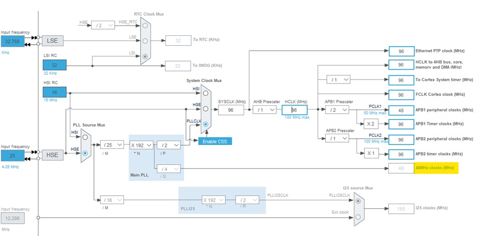
Figure 1: Clock Configuration for USB_OTG_FS
7.2. USB Peripheral Configuration in STM32CubeMX
After ensuring the clock is properly configured, proceed with setting up the USB OTG FS peripheral to handle USB communication at the hardware level.
7.2.1. Detailed Configuration Steps
-
Enable USB OTG FS:
- Within STM32CubeMX, navigate to Connectivity and select USB_OTG_FS.
- Set the mode to Device Only, as this will configure the STM32 to act as a USB device when connected to a host system such as a PC.
-
Set Up the USB Device Middleware:
-
Under Middleware, select USB_DEVICE. For serial communication over USB, choose the Communication Device Class (CDC), commonly referred to as Virtual COM Port. This selection enables the microcontroller to communicate with a host as if it were a standard serial port.
-
Customize the USB device descriptors (such as the
PRODUCT_String) within the Device Descriptor settings. These descriptors define how the USB device is identified by the host system, allowing for easier recognition and differentiation. -
Note: The USB_DEVICE middleware operates in conjunction with the
STM32_USB_DEVICE_Library, which houses the core USB functionality, referred to asusb_core. The core library manages fundamental USB operations but delegates higher-level communication protocols to other modules.
-
7.3. Memory Management: Adjusting the Heap Size
To ensure the microcontroller can handle USB communication efficiently, particularly when dealing with data buffers, it is necessary to adjust the default heap size.
7.3.1. Heap Size Adjustment
-
Increase Heap Size:
-
Access the Project Manager tab in STM32CubeMX. By default, the heap size may be set to 0x200 (512 bytes), which is often insufficient for USB operations.
-
Increase the heap size to 0x600 (1536 bytes). This additional memory allocation is crucial for accommodating the buffers required by the USB communication stack, ensuring smooth data transmission and reception.
-
To ensure the heap size has increased we can look at the linker script
/* Entry Point */
ENTRY(Reset_Handler)

/* Highest address of the user mode stack */
_estack = ORIGIN(RAM) + LENGTH(RAM);    /* End of RAM */

/* Define heap and stack sizes */
_Min_Heap_Size = 0x600;      /* Required amount of heap (1.5KB) */
_Min_Stack_Size = 0x400;     /* Required amount of stack (1KB) */

/* Specify the memory areas */
MEMORY
{
  RAM (xrw)      : ORIGIN = 0x20000000, LENGTH = 128K
  FLASH (rx)     : ORIGIN = 0x08000000, LENGTH = 512K
}
- Heap Size: Updated to
0x600(1536 bytes) to ensure sufficient memory for USB operations. - Stack Size: Maintained at
0x400(1024 bytes) to support typical stack usage scenarios.
7.4. Customizing USB Communication in usbd_cdc_if.c
To ensure that the device and the host computer agree on communication parameters such as baud rate, parity, and stop bits, the usbd_cdc_if.c file must be modified. This file also handles the reception of data from the USB interface.
7.4.1. Modifying Line Coding Commands
-
Storing Line Coding Information:
- To handle the Line Coding commands, add a variable of type
USBD_CDC_LineCodingTypeDefto store the communication settings.
In the block for adding private variables (
PV):/* USER CODE BEGIN PV */ /* Private variables ---------------------------------------------------------*/ USBD_CDC_LineCodingTypeDef LineCoding; /* USER CODE END PV */ - To handle the Line Coding commands, add a variable of type
-
Handling SET and GET Line Coding Requests:
- Modify the
CDC_Control_FSfunction to handleCDC_SET_LINE_CODINGandCDC_GET_LINE_CODINGrequests. This ensures the device correctly receives and responds to the host’s communication settings.
case CDC_SET_LINE_CODING: LineCoding.bitrate = (uint32_t)((pbuf[0]) | (pbuf[1] << 8) | (pbuf[2] << 16) | (pbuf[3] << 24)); LineCoding.format = pbuf[4]; LineCoding.paritytype = pbuf[5]; LineCoding.datatype = pbuf[6]; break; case CDC_GET_LINE_CODING: pbuf[0] = (uint8_t)(LineCoding.bitrate); pbuf[1] = (uint8_t)(LineCoding.bitrate >> 8); pbuf[2] = (uint8_t)(LineCoding.bitrate >> 16); pbuf[3] = (uint8_t)(LineCoding.bitrate >> 24); pbuf[4] = LineCoding.format; pbuf[5] = LineCoding.paritytype; pbuf[6] = LineCoding.datatype; break;- This implementation ensures that both the computer and the device agree on the communication parameters.
- Modify the
7.4.2. Handling Data Reception
-
Creating a Hook for Data Reception:
- Define a weak function
CDC_Receive_Handlerthat can be overridden to handle incoming data. This provides flexibility by allowing custom data handling outside of the default library implementation.
In the block for private function declarations:
- A weak function is only compiled if implemented; otherwise, all calls to it are ignored, which helps avoid unnecessary code execution.
__weak void CDC_Receive_Handler(uint8_t* pbuf, uint32_t *Len); - Define a weak function
-
Modifying
CDC_Receive_FSFunction:- Modify the
CDC_Receive_FSfunction to call theCDC_Receive_Handlerwhenever data is received. This ensures that received data is processed as soon as it arrives.
static int8_t CDC_Receive_FS(uint8_t* Buf, uint32_t *Len) { /* USER CODE BEGIN 6 */ USBD_CDC_SetRxBuffer(&hUsbDeviceFS, &Buf[0]); USBD_CDC_ReceivePacket(&hUsbDeviceFS); CDC_Receive_Handler(Buf, Len); /* <-- added here */ return (USBD_OK); /* USER CODE END 6 */ }- This function must execute quickly to ensure that the USB interface can continue processing incoming data without delays.
- Modify the
7.5. Finalizing the USB Communication Setup
Once the clock and peripheral configurations are complete, and the project code is generated by STM32CubeMX, the final step involves refining the generated code to suit your application’s specific needs.
7.5.1. Code Customization
-
Generated Code Overview:
- STM32CubeMX will generate several key files, including
usb_device.c,usbd_desc.c, andusb_cdc_if.c. These files contain the foundational code for USB communication, including initialization routines and descriptor settings.
- STM32CubeMX will generate several key files, including
-
Editing
usb_cdc_if.c:-
The file
usb_cdc_if.cis where the core data handling functions are implemented. This is the primary location for customizing how data is sent and received over USB. Modify these functions to align with your application’s communication protocol and data handling requirements. -
Middleware Structure:
usb_device.c: Manages the core USB device functionality.usbd_desc.c: Contains the USB device descriptors, which define how the device appears to the host.usb_cdc_if.c: Implements the interface for the CDC class, handling data transfers between the microcontroller and the USB host.
-
By carefully following these steps, you will configure a robust and efficient USB communication interface on your STM32 microcontroller. The process involves precise clock setup, enabling and configuring the appropriate peripherals, adjusting memory allocations, and customizing the generated code to meet your application’s specific needs. This comprehensive approach ensures reliable and high-performance USB communication, suitable for a wide range of embedded applications.
8. Configuring Analog Channels on STM32
Setting up analog channels on the STM32 microcontroller involves several key steps, particularly when configuring the ADC (Analog-to-Digital Converter) to read analog signals. This section will guide you through the process of declaring pins as analog inputs, configuring the ADC for optimal performance, and utilizing internal references such as the temperature sensor and voltage reference.
8.1. Selecting Analog Input Pins
Before proceeding with the configuration, it’s essential to identify which pins you will declare as analog inputs. This decision is crucial because changing the configuration later can be complex and may require reworking the hardware setup or significant software adjustments.
9. ADC Configuration
The ADC peripheral in STM32 microcontrollers is highly versatile, capable of converting multiple analog inputs simultaneously using DMA (Direct Memory Access) for efficient data handling. The following steps outline the configuration process:
-
Selecting ADC Channels (ADCx):
- Input Channels (INx): Choose the specific analog pins (INx) you intend to use as input channels. Each INx corresponds to a physical pin on the microcontroller.
- Internal Channels: Additionally, you can select internal channels such as the temperature sensor and the internal voltage reference (
Vrefint), which are invaluable for monitoring the microcontroller’s operating conditions.
-
Configuring DMA Settings:
- DMA Channel: Add
ADC1to the DMA settings. This will allow the ADC to transfer conversion results directly to memory without CPU intervention. - Data Width: Set the data width to “WORD” to ensure that each conversion result is stored in a 32-bit word format.
- Mode: Enable “Circular” mode for DMA. This mode allows continuous ADC conversions, where the DMA automatically restarts after each full transfer, ideal for real-time data acquisition.
- DMA Channel: Add
-
Adjusting ADC Parameters:
- Continuous Conversion Mode: Enable this mode to allow the ADC to continuously convert the selected channels without requiring additional triggers.
- DMA Continuous Request: Enable this to keep the DMA in sync with the continuous ADC conversions, ensuring that each conversion result is automatically transferred to memory.
- Number of Conversions: Set this parameter to the number of channels you have configured. This determines how many conversions the ADC performs before resetting.
- Clock Prescaler: Set the prescaler to divide
PCLK2by 4. Given our configuration with aPCLK2of 96 MHz, this results in an ADC clock of 24 MHz. - Sampling Time Calculation: To determine the conversion time, divide the number of cycles by the ADC clock. For example:
- 3 Cycles: 324 MHz=0.125 microseconds\frac{3}{24 \text{ MHz}} = 0.125 \text{ microseconds}24 MHz3=0.125 microseconds. This is extremely fast and might not be suitable for accurate conversions.
- 480 Cycles: 48024 MHz=20 microseconds\frac{480}{24 \text{ MHz}} = 20 \text{ microseconds}24 MHz480=20 microseconds. This is a more reasonable time, balancing speed and accuracy for most applications.
-
Implementing the ADC in the Main Program:
- After configuring the ADC, a handle (
hadc1) will be available in your main program. To store the ADC conversion results, declare a buffer:
uint32_t pData[2] = {0}; // Buffer to hold ADC conversion results- Start the ADC with DMA to begin storing conversion results in the buffer:
HAL_ADC_Start_DMA(&hadc1, pData, 2); // Start ADC with DMA, storing results in pData - After configuring the ADC, a handle (
10. Internal Voltage Reference (Vrefint)
The STM32 microcontrollers include an internal voltage reference (Vrefint), which is particularly useful for compensating for power supply variations or for calibrating measurements. According to the STM32 datasheet (Section 6.3.23), the typical value of Vrefint is 1.21V. You can use this reference to calculate the actual voltage of an input pin as follows:
voltage = value_pinA0 * 1210 / value_Vrefint; // Calculate voltage in mV
This formula assumes that value_pinA0 is the ADC reading of the target pin, and value_Vrefint is the ADC reading of Vrefint. The result gives you the pin voltage in millivolts.
10.1. Utilizing the Internal Temperature Sensor
The internal temperature sensor in STM32 microcontrollers is useful for monitoring the temperature of the microcontroller itself, which can be an indicator of ambient temperature or the device’s thermal performance. However, note that the sensor primarily measures the temperature of the silicon die, which may not reflect rapid ambient temperature changes due to the sensor’s thermal inertia.
10.1.1. Calculating Temperature
The temperature can be calculated using the following formula derived from the sensor’s characteristics:
\[ T= \frac{V_\text{temp} - V_{25}}{ \text{slope}} + 25 \]
Where:
- VtempV_{temp}Vtemp is the ADC reading of the temperature sensor.
- V25V_{25}V25 is the voltage corresponding to 25°C, typically 0.76V (as per Section 6.3.21 of the datasheet).
- The slope is the change in voltage per degree Celsius.
To implement this in code, assuming you are working in millivolts, the formula can be expressed as:
temp = ((V_temp * 3300) / 4095 - 760) * 1000 / slope + 25;
For the STM32, where the slope might be around 2.5 mV/°C, you could simplify this further:
temp = ((V_temp * 33000) / 4095 - 7600 + 25000) / 25;
This calculation yields the temperature in degrees Celsius, adjusting for the reference voltage and typical sensor characteristics.